A review of basic computer architecture follows, partially inspired by linux-insides. I originally wrote this in 2016, but made edits later.
Von Neumann Machines

Computers today are loosely based on the von Neumann architecture as shown above, with three major components – CPU, I/O devices, and memory – connected over buses (wires). The computer works as the CPU executes instructions that either read/write to memory, or interact with I/O devices.
Notably, this model applies to every piece of software running on a computer - they all get translated into machine instructions that the CPU carries out, which then interacts with other devices, which interacts with either more devices, or the human user. This includes every line of code in the BIOS, operating system, application, etc.
The following silly example gives a glimpse into the power of this simple model. Consider what happens between a keystroke and the letter getting displayed on the screen – say, in a web browser’s address bar.
- The circuit in the keyboard generates an interrupt to the CPU.
- The CPU invokes the corresponding interrupt handler implemented in the device driver. This handler contains hundreds, perhaps thousands, of assembly instructions. These instructions has been living on the hard disk after the OS install a long time ago, and got loaded into memory when the operating system started. Now they are being loaded into CPU cache lines and registers in order to be executed.
- Among other things, the instructions translate the keystroke into some keycode (which I believe is just ascii code, e.g. 0x41 for ‘a’) that represents the letter, and put the code inside a queue. The queue is a data structure contained in a utility library in the Linux kernel’s code base.
- There are system calls which, through several intermediate function calls, reads from that queue. The browser application, through several layers of abstractions of its own, is invoking one of those system calls reading from standard input.
- Upon receiving the input, the browser uses some graphics API (e.g. OpenGL) to call some graphics driver (e.g. Direct3D) in order to render the letter, passing in the letter’s code and the bitmap of the font to use.
- The graphics driver runs code on the CPU to tell the graphics card which pixels should be rendered in what color. The graphics card then renders it, and the monitor displays it.
- Along the way the browser also thoughtfully sent the search engine what you typed in order to give you auto-completions. This involves a slew of other CPU instructions and GPU rendering.
It’s rather amazing that this all works without much failure. Again, all of this is just CPU instructions plus interactions with other hardware – keyboard, main memory, graphics card, the monitor, etc. This mental model will be very useful when understanding what’s happening in the operating system of a computer.
Communication between CPU and Other Devices
A slightly more nuanced view of the architecture is that the CPU communicates with two different types of components: I/O and memory. Correspondingly there are roughly two different types communication channels: the northbridge and the southbridge. These are chipsets visible on a motherboard. The northbridge is closer to the CPU and responsible for communications requiring high performance (i.e. memory, and sometimes a video card), while all other devices go through the southbridge.

We now know the CPU talks to other components through ‘bridges’, but how exactly does the communication happen? What data is passed through and what kind of CPU instructions do we use?
CPU to Hardware: Memory-mapped I/O
One significant detail in the above diagram is that the only gateway the CPU has to the outside world is the front-side bus (FSB). Although this diagram is a bit outdated, the point still stands that, the primary interface between the CPU and the outside world is a bunch of pins on the FSB. These pins help transmit memory addresses and the data that’s read from / written to these addresses. So in terms of CPU instructions, the way you would use the CPU to communicate with the outside world is by issuing load and store instructions to memory locations.
Well, how does writing to the memory display things on the monitor?
That’s where memory-mapped I/O comes in. In x86, MMIO is the predominant way through which CPUs issue requests to other I/O devices. This mechanism maps device registers onto physical memory addresses, so that memory addresses do not just reference RAM – they can also reference things like video cards, BIOS, and other PCI extensions. When the CPU issues a memory instruction, the northbridge is responsible for routing it to the appropriate hardware via a memory address map. This map can be inspected with cat /proc/iomem under Linux. Here’s what shows up for me:
00000000-00000fff : reserved
00001000-00057fff : System RAM
00058000-00058fff : reserved
00059000-0009efff : System RAM
0009f000-0009ffff : reserved
000a0000-000bffff : PCI Bus 0000:00
000c0000-000ce5ff : Video ROM
000d0000-000d3fff : PCI Bus 0000:00
000d4000-000d7fff : PCI Bus 0000:00
000d8000-000dbfff : PCI Bus 0000:00
000dc000-000dffff : PCI Bus 0000:00
000f0000-000fffff : System ROM
00100000-bd158fff : System RAM
  02000000-02772d03 : Kernel code
  02772d04-02d1af3f : Kernel data
  02e77000-02fbbfff : Kernel bss
bd159000-bd15ffff : ACPI Non-volatile Storage
bd160000-bd5b9fff : System RAM
bd5ba000-bda00fff : reserved
bda01000-dd9a5fff : System RAM
dd9a6000-ddbb5fff : reserved
ddbb6000-ddbd5fff : ACPI Tables
ddbd6000-de0fefff : ACPI Non-volatile Storage
de0ff000-def5efff : reserved
def5f000-deffefff : reserved
defff000-deffffff : System RAM
df000000-dfffffff : RAM buffer
e0000000-feafffff : PCI Bus 0000:00
  e0000000-f1ffffff : PCI Bus 0000:01
    e0000000-efffffff : 0000:01:00.0
    f0000000-f1ffffff : 0000:01:00.0
      f1000000-f12fffff : efifb
  f6000000-f70fffff : PCI Bus 0000:01
    f6000000-f6ffffff : 0000:01:00.0
      f6000000-f6ffffff : nvidia
    f7000000-f707ffff : 0000:01:00.0
    f7080000-f7083fff : 0000:01:00.1
      f7080000-f7083fff : ICH HD audio
  ... (lots of PCI extensions)
fec00000-fec00fff : reserved
  fec00000-fec003ff : IOAPIC 0
fed00000-fed03fff : reserved
  fed00000-fed003ff : HPET 0
    fed00000-fed003ff : PNP0103:00
... (omitted)
I left out one important piece of hardware in the above paragraph – hard drives. Hard drives are a bit more complicated in that the CPU talks to them through yet another interface (e.g. ATA), and maybe Direct Memory Access (DMA) on top of ATA. DMA allows the hard disk controller to directly write to RAM, so that the CPU doesn’t have to keep polling from it and can read disk data from RAM as well. Ultimately though, the CPU accesses the hard disk just like anything else – by reading or writing to a memory location.
That covers how the CPU talks to other hardware. What about the other way around?
Hardware to CPU: Hardware Interrupts
Hardware interrupts are used by devices to notify the CPU that something happened which requires its attention. Typical examples include things like the disk controller saying the data the CPU is trying to read is ready, the keyboard saying a key was pressed, etc. There are both hardware and software interrupts, but we’ll focus on the hardware portion since that’s been the theme of this discussion. There are a lot more details on the Wiki page and the book Understanding the Linux Kernel.
Each interrupt is identified by a number between 0 and 255. Linux defines ranges within these 256 values that are dedicated to nonmaskable interrupts, maskable interrupts, and software interrupts. We don’t need to go into too much detail here. What’s more interesting is what exactly happens when an interrupt is issued.
On the hardware side, every hardware controller that can issue interrupts has an output line dedicated to interrupts. These lines are then connected to the input pins of a Programmable Interrupt Controller (PIC), which is in turn connected to special pins of the CPU. The PIC monitors its input lines for signals, translates them into a number between 0-255, and sends them over to the CPU through its special pin. The CPU would then stop what it’s currently doing and context switch to the appropriate interrupt handler. Here’s an overly simplified diagram stolen from the Internet showing this:
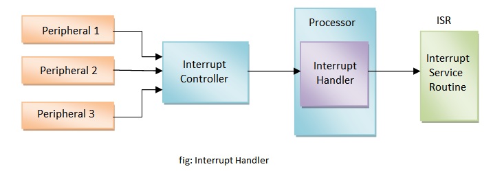
To know which interrupt handler to invoke, the CPU maps interrupt codes 0-255 to handlers with the Interrupt Descriptor Table (IDT). There is a special CPU register idtr that stores the address of the IDT. When an interrupt occurs, the CPU would just look up whatever is stored at the address this register points to for the interrupt handler. This means the IDT can be located anywhere in memory as long as its location is loaded into idtr appropriately, and this is exactly what the Linux kernel does. During the booting process, idtr is first initialized by the BIOS to point to a small interrupt table. Later Linux takes over and puts a new address into the register so it points to a more full-fledged IDT.